DIC Develops Resin for Resists Used in NIL, a Promising Next-Generation Semiconductor Fabrication Technology
- Business & Product
- News Release
Tokyo, Japan–DIC Corporation announced that has developed a resin appropriate for resists used in nanoimprint lithography (NIL), a technology that shows promise as a next-generation semiconductor fabrication process. The newly developed resin is based on an organic–inorganic hybrid polymer that leverages DIC’s world-class synthesis technologies. The Company began sample shipments of the resin to major device manufacturers several years ago, earning high marks from manufacturers as it worked toward commercialization.
The trend toward ever-smaller smartphones and other electronic devices with higher performance capabilities continues to drive efforts to fabricate semiconductors that achieve greater circuit integration through greater feature density. To date, efforts have centered on increasing feature density by improving photolithography, the most commonly used pattern-forming technology. However, with photolithography thought to have reached its theoretical limit in terms of feature density*, manufacturers and research organizations are exploring the potential of various next-generation fabrication technologies.
One of the most promising of these new technologies is NIL, in which patterns are formed by bringing a template (master mold) with nanoscale indentations into contact with an ultraviolet (UV)-curable resist layer that has been coated onto the substrate, pressing the template and the resist together and then curing the resist with UV light to create a high-precision etching mask that can be used to transfer the pattern to the underlying substrate. Because the etching mask is created by imprinting the template pattern directly onto the resist—unlike photolithography, in which patterning requires multiple intricate steps—NIL is attracting attention as a technology that significantly streamlines fabrication and reduces costs.
A principle concern with NIL has been the issue of pattern defects occurring when the template is removed from the resist after curing. Accordingly, considerable efforts have been allocated to the development of manufacturing equipment and materials that ensure defect-free release with the aim of solidifying NIL’s place as a next-generation fabrication technology and facilitating the formation of highly precise patterns.
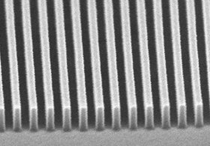
DIC’s new resin is based on a UV-curable organic–inorganic hybrid polymer, an area in which DIC has considerable specialized expertise. DIC improved durability during dry etching (i.e., resistance to reactive gases in the plasma used in the dry etching process), enhanced wettability and adhesiveness when coated on the substrate, and achieved excellent curing and release properties, thereby realizing a resin optimally suited for NIL.
In addition to developing this new resin, DIC has long worked to develop and apply technologies for achieving low metal ion levels with the aim of creating distinctive products for customers in the semiconductor industry. Today, DIC supplies these markets with a diverse range of highly rated products, including flourosurfactants with excellent leveling and release properties, which are used in a wide variety of leveling agents, as well as epoxy and phenolic resins boasting outstanding thermal resistance and durability during dry etching, which are used in resists and encapsulating materials.
Looking ahead, DIC will continue working to support customers in the semiconductor industry, which is seeing rapid technological innovation, by providing pioneering high-performance materials suited to cutting-edge fabrication processes.
* In photolithography, etching masks are created by transferring a circuit pattern from a photomask (a master plate made from silica or other transparent material) to a light-sensitive photoresist on the substrate by exposing it to light using a lithography device. The use of shorter wavelengths has made it possible to transfer patterns with higher feature density, but the 40 nm achieved with the argon fluoride (ArF) excimer laser is seen as photolithography’s limit. Multi-patterning technologies, which involve multiple lithographic exposures, have been commercialized for photolithography in response to demand for the further enhancement of feature density, the need for additional intricate steps pushes up fabrication costs.
—Ends—
PDF download
*Note: The files are in Adobe Acrobat Format. To view them you will need Acrobat Reader.


